
Sometime, I don’t know when, schematics stopped being a way to communicate how an electronic circuit works, and instead seem to have become the bare minimum needed for a PCB design.
For example, here is the schematic for the Adafruit Data Logger Shield for the Arduino open-source electronics platform.
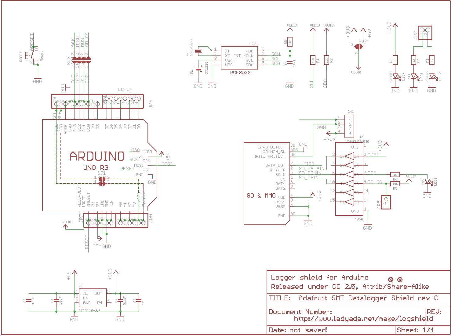
The schematic shows how the shield looks physically, and will provide a netlist for PCB design, but it’s a poor tool for conveying the intent and behavior of the design.
It takes some head scratching searching for net names and deciphering overlapping instance names just to glean what’s connected to what. In addition, while a number of jumpers make the shield more general purpose and can be conveniently used with different Arduino boards, there are no explanations!
The designer had the opportunity to make things simple for readers, but didn’t take advantage of it. Instead, we have to read the better half of a 68 page PDF companion document instead of having the information all in one place.
Here is a redrawn version of the same schematic.
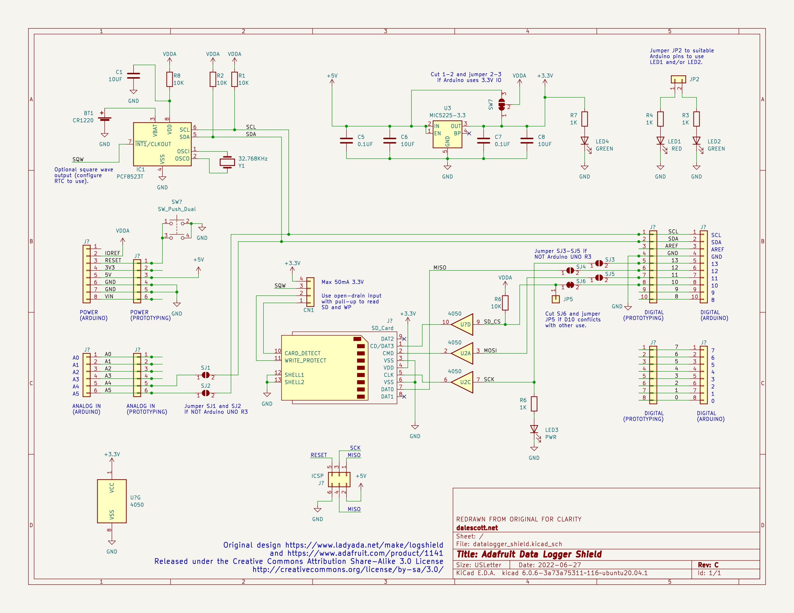
Granted it doesn’t have the same expanse of white space, but it provides an order of magnitude of more information. The primary circuit paths can be readily followed visually, component instances are legible, and there are comments to explain the purpose of the jumpers.
Given an opportunity to make things simpler for your audience, why would you instead make it harder?